In materials science, a surface interface refers to the boundary region between air or a vacuum and physical media. The atomic composition and topography of a solid’s surface monolayer can determine many of the chemical-mechanical characteristics of the bulk material, including solid—gas interfaces such as adsorption and permeation. Reaction kinetics of catalysts and the electromechanical performance of semiconducting materials for thin film fabrication are both affected by surface interface phenomena.
Modern surface engineers consider surface interface analysis a critical stage of development and process control. This article will explore how surface interface analysis is performed in more detail, while highlighting some of its critical applications:
Secondary Ion Mass Spectrometry for Surface Interface Analysis
Surface interface analysis is carried out in ultra-high vacuum (UHV) conditions with a primary ion source. This setup doses a solid sample with varying ion levels. These primary ions sputter the surface and cause atoms to collide, recoil, and collide again. This cascading process causes an energetic release of solid material, and though the primary ions may sputter through several physical layers up to nanometer depths, ejected material comes almost exclusively from the surface. With fully-tunable oxygen or argon ion guns, it is possible to restrict the ionization of surface particles to the uppermost monolayer.
Ionized atoms or molecules eject from the uppermost monolayer and are detected by the ion optical acquisition component of the quadrupole mass spectrometer. This process is termed secondary ion mass spectrometry (SIMS), and is one of the key methodologies for high purity material characterization through surface interface analysis.
SIMS is considered the most sensitive analytical technique for acquiring data relating to the nanometric composition of a solid sample’s uppermost surface layers and its surface interface properties. Detection is on the sub parts per billion (ppb) scale. This technique can be performed for surface interface analysis of ceramic materials, polymers, semiconductors, and biological matter, providing a broad range of quantifiable mass spectral information.
Surface interface analysis that is carried out to this outstanding degree of specificity can be used to determine the electrochemistry of semiconducting materials and predict the performance of electron—hole pair transportation in thin film structures. It can also be used to determine the chemisorption properties of sputter targets in magnetron sputtering and chemical vapor deposition (CVD), to reduce the effects of detrimental column tilt.
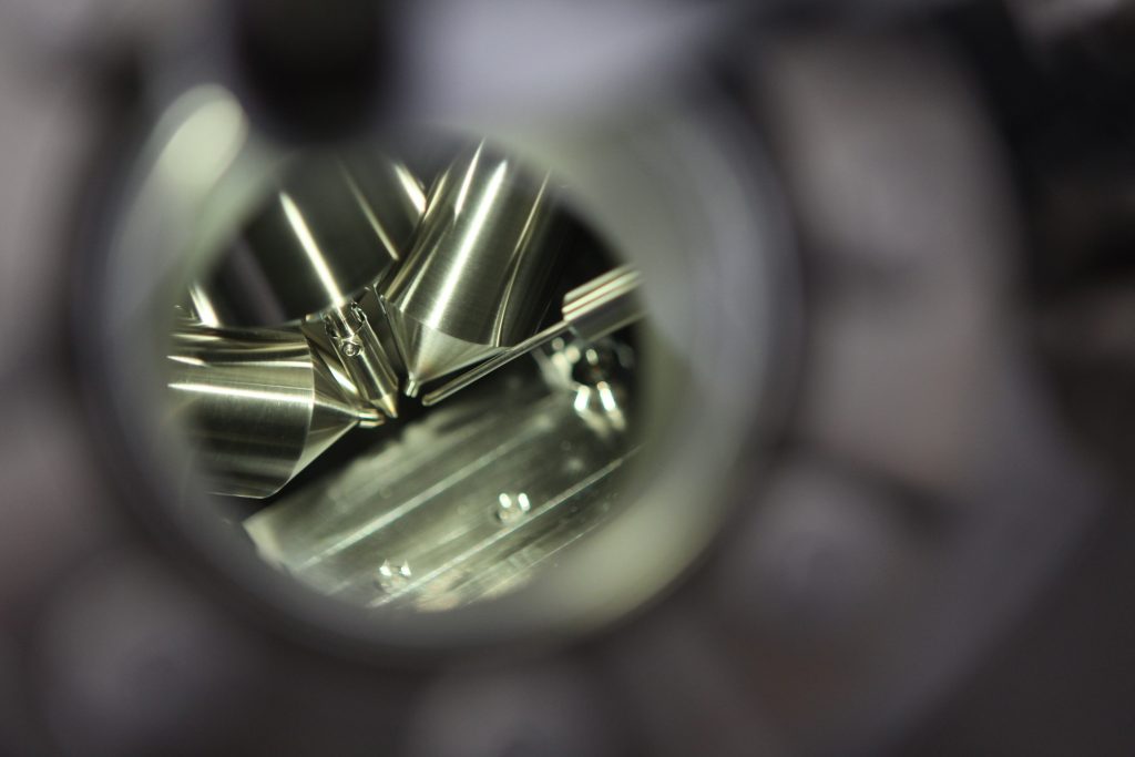
The Hiden Compact SIMS tool provides rapid elemental characterization of a material’s surface composition and topography, providing finely-tuned experiment parameters for unique surface interface analysis processes. An IG20 oxygen / argon ion gun can be adjusted to a spot size of just 50 microns for static and dynamic secondary ion analysis. Static analysis is preferable for surface interface analysis as it provides a low dose of primary ions for sampling the uppermost monolayer of solid matter with low overlapping of collision cascades from layers below the surface. This tool has been used for surface interface analysis in thin film fabrication, geochemical characterization, glass coating assessments, and more.
Surface Interface Analysis with Hiden Analytical
At Hiden Analytical, we have prepared a broad range of products and techniques to ensure that you can assess materials at the level that you require. Surface interface analysis is a cutting-edge form of materials characterization and process control, requiring the most accurate ion detectors and pure sample chambers for providing actionable data.
If you would like any more information about performing surface interface analysis with our quadrupole mass spectrometers, please do not hesitate to contact us.