DC Magnetron Deposition of SiBCN Films

DC Magnetron Deposition of SiBCN Films for Enhanced Microelectronics Performance
At Hiden Analytical, we are committed to advancing microelectronics technology by providing cutting-edge solutions for material deposition.
Related Products
At Hiden Analytical, we are committed to advancing microelectronics technology by providing cutting-edge solutions for material deposition. One such innovative material is the silicoboron-carbonitride (SiBCN) film, which boasts a unique combination of properties that make it an ideal choice for various microelectronics applications. DC magnetron sputtering is the preferred method of depositing these films, as it offers enhanced electronic capabilities and improved film properties.
Key Advantages of SiBCN Films
- Extremely high temperature stability and oxidation resistance
- Low thermal coefficient of expansion
- Low thermal conductivity
- High hardness and creep resistance even at elevated temperatures
- Reduced film stresses and good substrate adhesion

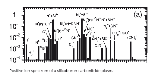
Positive ion spectrum of a siliconboron-carbonitride plasma
Hiden EQP: Advanced Plasma Analysis for SiBCN Film Deposition
The Hiden EQP system was employed to investigate the composition of the plasma during the DC magnetron deposition of SiBCN films. By analyzing the plasma directly, the Hiden EQP allows for a better understanding of the relationship between plasma conditions and the resulting film properties. This in-depth analysis enables the optimization of gas composition, power, and substrate temperature during deposition.
Amorphous SiBCN Films with Exceptional Properties
Using the Hiden EQP system, the deposited SiBCN films were found to have an amorphous structure, which contributes to their remarkable properties. These films exhibit:
- High hardness
- Low surface roughness
- Excellent oxidation resistance at elevated temperatures up to the substrate limit of 1350°C
At Hiden Analytical, we are dedicated to providing the best in plasma analysis technology to ensure the highest quality film deposition for microelectronics applications. Our advanced EQP system is designed to help you achieve optimal results with SiBCN films and other advanced materials. Contact the Hiden Analytical team today to learn more about our Solutions for your Microelectronics.
Atmospheric Plasma Analysis by Molecular Beam MS – GEC 2004 (1.38 MB)
Atmospheric Pressure Plasma Analysis by Modulated Molecular Beam MS – ICPIG 2005 (256 KB)
Ion Energy Distributions for a DC Plasma – GEC 2003 (250 KB)
Mass Analysis of CF3I Decomposition in a Surface Barrier Discharge – GEC 2011 (2.8 MB)
Mass Spectroscopy of Metastable Species during Plasma Processing – GEC 2011 (2.1 MB)
Time Resolved Ionisation Studies of HIPIMS – PSE 2006 (848 KB)

