Structures with length scales numbered in a quantity of atoms from roughly 1 – 100 nanometres (nm), or below the mesoscopic scale, are characterized as nanoscale materials. The nanomolecular properties of macro-structures can be assessed through nanoscale depth profiling and elemental surface mapping, which conventionally use focussed ion beam (FIB) or secondary ion mass spectrometry (SIMS).
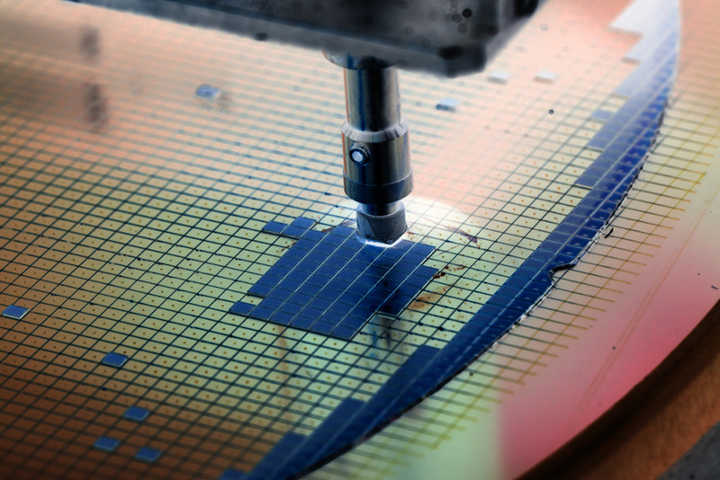
FIB systems can modify the surface of a sample material by sputtering the substrate with an incident beam of ions. This can be used to remove or deposit material as appropriate. To acquire nanoscale depth profiles and map the elemental surface composition of samples, FIB sputtering must be combined with advanced extraction optics such as a scanning electron microscope (SEM) or a quadrupole mass spectrometer.
Outlining FIB-SIMS
The Hiden EQS is a high transmission SIMS detector optimised for surface analysis of materials by ion energy, and low ion extraction field optics. It is uniquely attractive as an after-market, or bolt-on energy detector for FIB microscopes due to the device’s axial collection of ions. Combining these devices represents significant improvements for nanoscale depth profiling of samples with outstanding elemental detection limits down to the parts per million (ppm) range.
FIB-SIMS is used to generate high resolution nanoscale depth profiles through secondary ion sputtering. The primary focussed ion beam of the FIB microscope scans the surface of the sample and the EQS detector obtains the ejected secondary ions with a high dynamic range of up to six orders of magnitude. This enables the system to assess multiple species expelled via sputter erosion, including positive and negative ions, with enhanced lateral resolution of 50 nm.
Once charged particles have been acquired by the EQS detector, they pass through a 45° sector analyser that can measure energy at increments of 0.5 eV. The energy resolved ions then pass through a quadrupole mass spectrometer for elemental analysis across a range of up to 5000 amu, with configurations available for light element analysis, lithium for example.
This analytical technique surpasses SIMS in terms of lateral analytical resolution and provides superior elemental mapping for analysis of trace elements in nanoscale structures. This includes commercial and industrial semiconductor products as well as organic geological samples. Nanoscale depth profiles of meteoritic rock through FIB-SIMS, for example, enabled analysts to assess the composition of distinct zircon (ZrSiO4) grains in a sample to determine the genesis of the material.
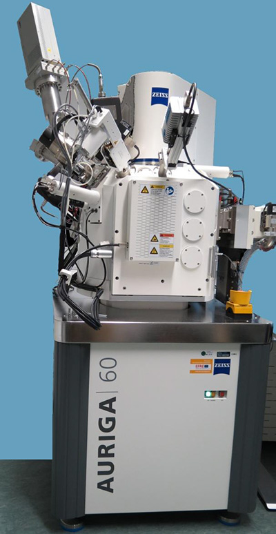
FIB-SIMS instrumentation is available for a range of conventional microscopes, including:
- 15xx Series
- AURIGA Series
- NEON Series
- XB 340 & XB 350

FIB-SIMS with Hiden Analytical
Hiden Analytical supplies high-precision mass spectrometry solutions for some of the most advanced surface science applications worldwide. Nanoscale depth profiles of novel structures with sub-micron dimensions is possible with FIB-SIMS, providing detailed 3D representations of the mass and energy resolved particles from a sputtered sample. It is also possible to assess the uppermost monolayer of structures on the macroscale with highly precise control of the incident focused ion beam, for nanoscale depth profiles of commercial products such as low emissivity architectural glass.
The SIMS system is designed to enhance the capacities of an existing FIB system to provide precise elemental imagery across the existing systems entire field of view.
If you would like any more information about acquiring superior nanoscale depth profiles and elemental surface maps with your existing FIB system, please do not hesitate to contact us.

