Surface engineering refers to a branch of materials science with an enormous range of applications and methodologies – many of which have been implemented since before the terminology ‘surface engineering’ was widely adopted. The treatment and laying of compressed gravel or cobblestones to create hardened surfaces on top of designated roadways is a process that spans millennia, representing the very definition of surface engineering: altering the surface or substrate of a material to optimize its utility and application. Similar processes for treating macro-products are still used today, but modern surface engineering is increasingly concerned with altering products on a microscopic scale.
Thin film materials are layered nanostructures ranging from a few nanometers (nm) to micrometer (μm) dimensions. They are formulated through a multitude of methodologies, including:
- Atomic layer deposition (ALD);
- Chemical vapor deposition (CVD);
- Ion beam etch (IBE);
- Magnetron sputtering;
- Metal organic chemical vapor deposition (MOCVD);
- Molecular beam epitaxial growth (MBE);
- Plasma reactive ion etch (RIE);
- Reactive ion beam etch (RIBE).
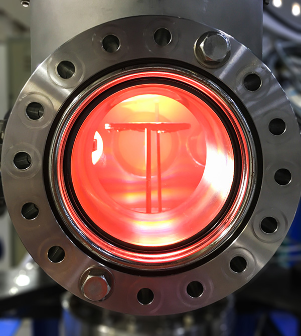
These processes are applied to manipulate and alter the substrates of materials on an atomic scale, changing and optimizing its mechanical or chemical properties. ALD surface engineering techniques, for example, are commonly used to coat the substrate of lithium batteries with thin film coatings designed improve mechanical stability and encourage electron movement between cathodes and anodes. Chemical vapor deposition techniques meanwhile are often used for surface engineering of transparent or reflective materials, with common applications for the formation of optical bandpass filters or architectural glass.
Each of these techniques is a sensitive mechanical process that occurs within pre-defined chemical parameters. It is crucial that distinct conditions are met and maintained to ensure that thin film products can be manufactured efficiently, and with repeatable results. One of the primary methods for controlling these process methods is to administer mass spectrometry equipment capable of monitoring specific mass-related metrics in thin film processing equipment.
Mass Spectrometers for Thin Film Surface Engineering
Multiple Hiden Analytical mass spectrometers are used for quality control of thin film surface engineering procedures. They can be used to support the development and manufacture of products such as organic photovoltaic cells, emerging digital devices, innovative automotive solutions, and technological textiles.
Thin film optical coating processes, for example, can be monitored through residual gas analysis (RGA) methods using the HPR-30 RGA mass spectrometer. It is configurable for analysis of gas and vapor, providing rapid real-time analysis of thin film deposition methods, including CVD. In CVD surface engineering, it is important that specific pressures and atmospheric compositions are sustained to ensure high throughput production of optical equipment with distinct characteristics. Optical filters are typically required to block specific wavelengths of light, so must be finely configured with distinct bandpass characteristics. The HPR-30 can support the development of optical thin films by providing accurate leak and contamination detection analysis for CVD surface engineering processes.
If you would like any more information on using a Hiden Analytical mass spectrometer for surface engineering of thin film materials, please do not hesitate to contact us.