Thin-film CdTe solar cells boast lab-scale efficiencies above 20% when designed in the ‘superstrate configuration’ whereby the transparent front electrode is deposited first, on a glass superstrate. By inverting the design so that the front electrode is deposited last (i.e. the ‘substrate’ configuration), the cells can be fabricated on lightweight, flexible metal foils, thereby widening the range of possible applications. Here, ITO/CdS/CdTe/Mo solar cells have been grown in the substrate configuration by a combination of close-space sublimation and RF sputtering. A two stage CdCl2 post-growth annealing process was developed, with the first stage contributing to CdTe doping and the second being linked to CdTe/CdS inter-diffusion. The inter-diffusion process was monitored using a Hiden Analytical secondary ion mass spectrometry (SIMS) system. Modelling of device performance predicts efficiencies as high as 11.3% may be obtainable upon formation of an Ohmic back-contact.
Substrate CdTe solar cells were processed as follows: on Mo foil substrates, p-type CdTe films (1.8 – 10 μm) were close space sublimation-deposited, from a powdered source. Then, by RF sputtering, n-type CdS window layers (200 nm) and the ITO front contact layers (200 nm) were deposited. Preliminary testing indicated that the standard CdCl2 annealing process used for superstrate devices (typically a 20 min anneal of the CdS/CdTe stack at 420°C following CdCl2 evaporation) was ineffective for substrate cell activation. Hence, in order to optimize the device processing, different CdCl2 post-growth treatments were tested: Treatment A) a single air-anneal at 420°C following CdCl2-deposition onto CdS/CdTe stacks; Treatment B) a single air-anneal following CdCl2-deposition onto just the CdTe layer, but before CdS deposition; and Treatment C) identical to treatment B, but with a second air-anneal (480 – 580°C) introduced after ITO/CdS deposition.
Figure 1 shows the current-voltage (J-V) curves of the best performing ITO/CdS/CdTe/Mo devices obtained from each of the post-growth treatments. All devices subject to post-growth treatment A performed poorly, the majority of contacts were short-circuits while the remainder typically had η < 0.5%. Devices subject to post-growth treatment B, also performed poorly, with the highest efficiency achieved being η = 1.96%. Post-growth treatment C however (twice-annealed) yielded significant performance enhancements (η ~ 5 – 6%), principally as a result of enhancements to VOC and FF, implying an improvement in junction quality. A peak efficiency of 8.01% was finally achieved using treatment C upon incorporating a ZnO buffer layer between CdS and ITO (see Paper reference); this represents the best Cu-free substrate CdTe device reported. Whilst the first annealing stage, i.e Cl-activation of the CdTe layer, is known to enhance p-type doping of CdTe, the impact of the second annealing stage on the composition of the stacks was investigated using SIMS profiling. Two devices were analysed, one having been annealed once (Treatment B, η = 1.96%) and one having been annealed twice (Treatment C, η = 6.05%). Figure 2a shows that S diffusion into the CdTe layer is enhanced by the second anneal: Inter-diffusion of S and Te is thought to assist in the passivation of surface defects at the interface and therefore lead to reduced interface recombination. The improvements in VOC and JSC affected by the second annealing step are consistent with this. Figure 2b shows there is also a distinct difference in the Cl-profiles of the two devices: In the device subject to two annealing stages (C) there is a higher Cl concentration in the CdS layer and in the bulk of the CdTe, and this is likely to induce beneficial morphological changes in the junction region, i.e. recrystallization of both materials to minimise strain. It is evident that, for effective activation of substrate cell devices, a two-stage annealing process is necessary. This work is to be continued at the Stephenson Institute for Renewable Energy by Dr. Jon Major within the UK Photovoltaic Centre for Doctoral Training.
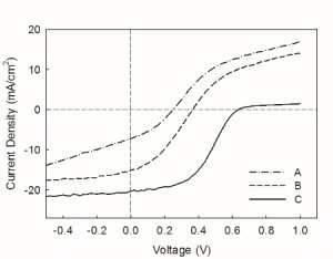
Figure 1: Current-voltage (J-V) curves of substrate configuration CdTe solar cells, obtained after applying different post-growth CdCl2-treatments, A–C. *Modified from the paper reference.
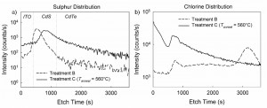
Figure 2: SIMS depth profiles of S- and Cl- in ITO/CdS/CdTe stacks that were subject to treatment B (single-anneal) and treatment C (double-anneal). The left edges of the plots represent the front surfaces of the cells, i.e. the ITO surfaces.
Project Summary by:
Benjamin L. Williams
Dept. of Applied Physics
Eindhoven University of Technology
P.O. Box 513, 5600 MB Eindhoven
The Netherlands ()
*Address at time research was carried out:
Stephenson Institute for Renewable Energy
University of Liverpool, L69 7ZF
United Kingdom
Corresponding author:
Jon D. Major
Stephenson Institute for Renewable Energy
University of Liverpool, L69 7ZF
United Kingdom ()
Reference:
B.L. Williams , J.D. Major, L. Bowen, L. Phillips, G. Zoppi, I. Forbes, K. Durose (2014), “Challenges and prospects for developing CdS/CdTe substrate solar cells on Mo foils” Sol. Energy Mat. & Sol. Cells. doi:10.1016/j.solmat.2014.01.017
Visit Product Page : IG20
View Full Newsletter : Mass Spectrometers for UHV Surface Science
Make an enquiry : Send us a message