Quadrupole mass spectrometry is used extensively in the electronics sector to assess the functionality of surface materials and the performance of thin film structures. The surface interface characteristics of these materials are integral in optimising the macrostructural properties of an optoelectronic device. Topographical defects in the glass coating of an organic photovoltaic (OPV) solar cell could impact the light-attenuation capabilities of junctions in the electronic structure, for example. Small variations in an optical coating could cause light to reflect rather than propagate through the substrate and be converted into electricity.
How to analyse the top nano layers of a material is a key question for manufacturers of electronic devices as their functionalities continue to grow more complex. Novel solar cells comprised of multi-junction nanocrystals are already beginning to display enhanced solar energy conversion over conventional p-n junction silicon OPVs. However, these structures must be subject to rapid and reliable quantitation on the nanoscale to optimise their surface interfaces and provide justification for the new technology from a cost and efficiency perspective.
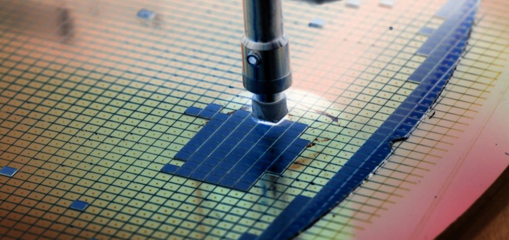
Secondary Ion Mass Spectrometry (SIMS) is the leading method for analysing the top nano layers of a material in the electronics sector. It is routinely used for post process analysis of thin film devices for quality control and quality assurance purposes. It provides a novel answer for how to analyse the top nano layers of a material through non-invasive means.
How to Analyse the Top Nano Layers of a Material with SIMS
SIMS technology operates using an incident ion beam that sputters the uppermost monomolecular layers of a sample material and analyses the ionised atoms that have been ejected from the substrate. These ions are detected and quantified to provide high resolution depth profiles and reliable surface imagery.
The Hiden SIMS family of instruments are based on this fundamental principle, offering high sensitivity detection of elements, molecules and isotopes with nanometre depth resolution. Each system is optimised for different application requirements, from economical and routine laboratory analysis to full-featured ultra-high vacuum (UHV) surface interface assessments. The range is comprised of:
- Compact SIMS: providing rapid surface analysis with a novel, low footprint design. It is uniquely suited for lower footprint facilities looking at how to analyse the top nano layers of a material effectively and economically.
- AutoSIMS: is a fully-automated surface analysis tool that has been optimised for high throughput testing during long periods of operation. It offers the full suite of SIMS capabilities, including detailed surface spectra and 2D or 3D depth profiling.
- SIMS Workstation: a robust solution for static and dynamic surface composition analysis and depth profiling. It is an easily-customisable system with additional components available for specialised applications.
Surface Analysis with Hiden Analytical
At Hiden Analytical, we recognise the challenge of how to analyse the top nano layers of a material in varied laboratories and manufacturing environments. The SIMS technique is the leading method of surface analysis for electronics manufacturing and research and development, with a suite of software solutions and a range of additional products available as required.
If you would like any more information about how to analyse the top nano layers of a material with particular budgeting or analytical requirements, simply contact us for more details.