Nanotechnology represents a new frontier in research and development (R&D) across a broad spectrum of human endeavours. Though concerned with the miniscule, the scope of nanotechnology is undeniably vast. However, most of the exciting nanoscience research being conducted is in a purely contemplative phase – or at least an extended period of prototypical development.
The Reality of Modern Nanotechnology
Consider graphene: A monomolecular allotrope of carbon that was first isolated from graphite via physical exfoliation over a decade ago. Though remarkable as the first atomically thick substance ever engineered, media hyperbole regarding next-generation applications of graphene have largely proven fruitless. That isn’t to say that graphene hasn’t been successfully functionalised, just that the realm of nanotechnology has a fair way to go before the likes of magnetic medicine and quantum computing become our new reality.
One of the few functional successes of nanoscience to date is the thin film. Though there is no singular definition of thickness that constitutes a thin film, they typically deal with coatings that are no thicker than a few micrometres (μm). Manufacturers are increasingly able to deposit precise thin coatings of just a few nanometres (nm) due to improvements in process sophistication and quality. This advanced method of surface engineering has proven essential to the ongoing ingenuity of manufacturers and researchers in a range of fields.
Cutting-Edge Surface Engineering
Select coating processes, such as atomic layer deposition (ALD), have pushed the boundaries of thin film nanotechnology by enabling the production of conformal films with tight control of both composition and thickness at the atomic range. By selectively and sequentially introducing precursor gases into an ALD vacuum chamber, complex substrates are exposed to individual gas phases in a series of alternating cycles. Gas molecules precipitate on the target surface in a self-limiting manner, which means reactions cease as soon as all reaction sites are occupied. Theoretically, this yields a precisely uniform, extremely thin coating of precipitate which acts as the new reaction surface for subsequent gas phase molecules.
ALD is envisaged as one of the greatest processes for electronic device miniaturization, next-level integrated circuit (IC) density, and novel energy storage systems. However, it is not a singular process and is instead used as an umbrella term to encompass a broad framework of systems that operate on these basic surface engineering principles.
Thin Films & Nanomaterials Today
Yet, even as mankind’s chemical surface engineering efforts continue to push towards the atomic scale, research at the nano-, micro- and even macroscales are continuing to pay dividends in terms of nanotechnological progress.
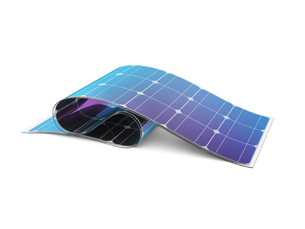
Vacuum-rated crystal growth furnaces are increasingly used to develop high-purity semiconducting alloys such as gallium arsenide or indium phosphide, both critical contenders for high bandgap multijunction photovoltaics – also known as tandem solar cells. These are generated epitaxially, much like conventional silicon, but offer dramatically improved quantum efficiency and performance.
We are also beginning to see the increased application of nanocrystals in the form of quantum dots (QDs); electro- and photoluminescent materials that are mainly used in display applications due to their outstanding spectral characteristics. Materials like QDs are expected to form part of the backbone of the display and lighting market in the coming years, even as scientists continue to explore novel uses of synthesised nanocrystals such as energy generation and nanomedicine.
Carefully engineered micro-electromechanical systems (MEMS) based on thin films on the order of micrometres are similarly pushing the technological letter in the field of telecommunications, as ultrafast 5G networks continue to rollout across the world.
Learn more about Surface Engineering of Thin Film Materials
At Hiden Analytical, we develop and deliver high-performance quadrupole mass spectrometry solutions for a broad range of application areas including, real time gas analysis, vacuum process monitoring, plasma ion and radical analysis and thin film surface analysis at the nanometre scale. Our mass spectrometry tools provide an understanding of the processes involved in nano-material science enabling the next generation of discovery. Our experience with nanoscience and technology is unprecedented, as we routinely offer systems for quality assurance and control (QA/QC), gas analysis, vacuum diagnostics, and much more. If you have any questions about our mass spectrometry systems for nanotechnology applications, simply contact a member of the team today.