Semiconductors are critical materials in electronics manufacturing, displaying unique electrical conductivity properties that fall between the values of insulators and conductors. Silicon (Si) is a ubiquitous semiconductor that is widely used in the fabrication of microprocessors and thin film structures including hard-disks and solid-state drives, handheld digital devices, and solar photovoltaic cells. These devices must be pervasively assessed using mass spectrometers to ensure high-degrees of device functionality are sustained across multiple production batches.
 RGA Mass Spectrometers for Doping Analysis
The unique electronic behaviour of silicon (Si) is explained by the atomic arrangement of electrons in its outer orbit which can be altered through chemical doping to decrease the material’s electrical resistance. Intrinsic semiconductors such as silicon display crystalline forms of covalently-bonded atoms in its outer orbital shell. Deliberately introducing impurities such as phosphorous (P) or gallium (Ga) into the material’s physiochemical structure adds free electrons into the system to enable electrical conduction. This process requires absolute chemical purity to reduce the risk of mechanical defects in the substrate wafer.
Residual gas analysis (RGA) is routinely used in silicon doping to monitor contaminants in ultra-high vacuum process chambers and to analyse process gases for optimal chemical content and distribution across silicon substrates. The RGA Series of mass spectrometers are extensively used throughout semiconductor manufacturing, for applications including atomic layer (ALD) and chemical vapor deposition (CVD) processes, with high sensitivity to gaseous reaction products, contamination and for leak detection.
SIMS Mass Spectrometers for Surface Depth Profiling
After a silicon wafer has been suitably augmented with dopants to display the requisite electrical resistance characteristics, it is treated through one of several different coating processes. Photolithography and photoetching are among the most common surface engineering methods used to develop nanoscale integrated circuits on semiconducting substrates by coating the surface with a light-sensitive material and applying a photoresistive mask to generate electronic patterns.
RGA Mass Spectrometers for Doping Analysis
The unique electronic behaviour of silicon (Si) is explained by the atomic arrangement of electrons in its outer orbit which can be altered through chemical doping to decrease the material’s electrical resistance. Intrinsic semiconductors such as silicon display crystalline forms of covalently-bonded atoms in its outer orbital shell. Deliberately introducing impurities such as phosphorous (P) or gallium (Ga) into the material’s physiochemical structure adds free electrons into the system to enable electrical conduction. This process requires absolute chemical purity to reduce the risk of mechanical defects in the substrate wafer.
Residual gas analysis (RGA) is routinely used in silicon doping to monitor contaminants in ultra-high vacuum process chambers and to analyse process gases for optimal chemical content and distribution across silicon substrates. The RGA Series of mass spectrometers are extensively used throughout semiconductor manufacturing, for applications including atomic layer (ALD) and chemical vapor deposition (CVD) processes, with high sensitivity to gaseous reaction products, contamination and for leak detection.
SIMS Mass Spectrometers for Surface Depth Profiling
After a silicon wafer has been suitably augmented with dopants to display the requisite electrical resistance characteristics, it is treated through one of several different coating processes. Photolithography and photoetching are among the most common surface engineering methods used to develop nanoscale integrated circuits on semiconducting substrates by coating the surface with a light-sensitive material and applying a photoresistive mask to generate electronic patterns.
 Secondary ion mass spectrometry (SIMS) uses a miniscule bombardment of primary ions to analyse the uppermost layers of a substrate material. SIMS mass spectrometers are widely used to assess depth profiles of ion implants, as well as depth profiles of multi-layered stacks, MBE MOCVD (molecular beam epitaxy metal oxide carbon vapour deposition), or magnetron sputtered grown layers for example. SIMS depth profiling reveals the atoms/cc as a function of depth in an implant. For multilayer stacks, SIMS reveals the degree of diffusion between layers providing vital information on the growth process quality. A complimentary technique to SIMS is Temperature programmed desorption (TPD). The TPD Workstation measures desorbing species as a function of temperature from samples at UHV from ambient temperature up to a maximum 1000°C with rapid data acquisition of up to 500 data points per second. The TPD profile data reveal further details of the thin film growth process.
Plasma Characterisation for Semiconductor Etching
Photoetching typically follows lithographic printing in the semiconductor engineering process. The silicon wafer is bombarded by charged or neutral plasma in a low-pressure chamber to alter the surface properties of the photolithographically printed integrated circuit. Etch gas sources vary, with atoms, photons, and radicals interacting with the surface material of silicon wafers.
Plasma ion analysis is critical for determining the interactivity between a plasma etch source and the chemical composition of the coated silicon wafer. The EQP mass spectrometer system is used to assess the reaction kinetics of plasma sources and diagnose process conditions. The combination of ion energy analyser and mass spectrometer provides for simultaneous mass and energy analysis providing vital information relating to the etch process including etch end point detection. Ion energy information is used to optimise the plasma etch source for an effective etch rate with low damage. The EQP system features a differentially-pumped triple filter quadrupole mass spectrometer with mass range of 300 amu as standard, with a wide range of mass range options including up to 5000 amu for plasma cluster and polymerisation studies. The EQP ion energy analyser has an ion energy range of 100eV as standard. 1000ev ion energy range is offered as an option for energetic plasmas.
Mass Spectrometers from Hiden Analytical
Hiden Analytical has engineered leading mass spectrometers for a broad range of industrial applications, supporting innovation in some of the world’s most cutting-edge fields. Our instruments are used at every stage of semiconductor processing and manufacturing by some of the most advanced semiconductor manufacturers and researchers on earth.
If you would like any more information about our mass spectrometers, please do not hesitate to contact us.
[Featured image courtesy of Saha Institute of Nuclear Physics]
Secondary ion mass spectrometry (SIMS) uses a miniscule bombardment of primary ions to analyse the uppermost layers of a substrate material. SIMS mass spectrometers are widely used to assess depth profiles of ion implants, as well as depth profiles of multi-layered stacks, MBE MOCVD (molecular beam epitaxy metal oxide carbon vapour deposition), or magnetron sputtered grown layers for example. SIMS depth profiling reveals the atoms/cc as a function of depth in an implant. For multilayer stacks, SIMS reveals the degree of diffusion between layers providing vital information on the growth process quality. A complimentary technique to SIMS is Temperature programmed desorption (TPD). The TPD Workstation measures desorbing species as a function of temperature from samples at UHV from ambient temperature up to a maximum 1000°C with rapid data acquisition of up to 500 data points per second. The TPD profile data reveal further details of the thin film growth process.
Plasma Characterisation for Semiconductor Etching
Photoetching typically follows lithographic printing in the semiconductor engineering process. The silicon wafer is bombarded by charged or neutral plasma in a low-pressure chamber to alter the surface properties of the photolithographically printed integrated circuit. Etch gas sources vary, with atoms, photons, and radicals interacting with the surface material of silicon wafers.
Plasma ion analysis is critical for determining the interactivity between a plasma etch source and the chemical composition of the coated silicon wafer. The EQP mass spectrometer system is used to assess the reaction kinetics of plasma sources and diagnose process conditions. The combination of ion energy analyser and mass spectrometer provides for simultaneous mass and energy analysis providing vital information relating to the etch process including etch end point detection. Ion energy information is used to optimise the plasma etch source for an effective etch rate with low damage. The EQP system features a differentially-pumped triple filter quadrupole mass spectrometer with mass range of 300 amu as standard, with a wide range of mass range options including up to 5000 amu for plasma cluster and polymerisation studies. The EQP ion energy analyser has an ion energy range of 100eV as standard. 1000ev ion energy range is offered as an option for energetic plasmas.
Mass Spectrometers from Hiden Analytical
Hiden Analytical has engineered leading mass spectrometers for a broad range of industrial applications, supporting innovation in some of the world’s most cutting-edge fields. Our instruments are used at every stage of semiconductor processing and manufacturing by some of the most advanced semiconductor manufacturers and researchers on earth.
If you would like any more information about our mass spectrometers, please do not hesitate to contact us.
[Featured image courtesy of Saha Institute of Nuclear Physics]
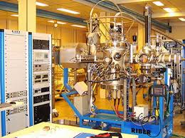
Riber SA MBE system with Hiden HALO 201 MBE residual gas analyser – photo courtesy of Saha Institute of Nuclear Physics
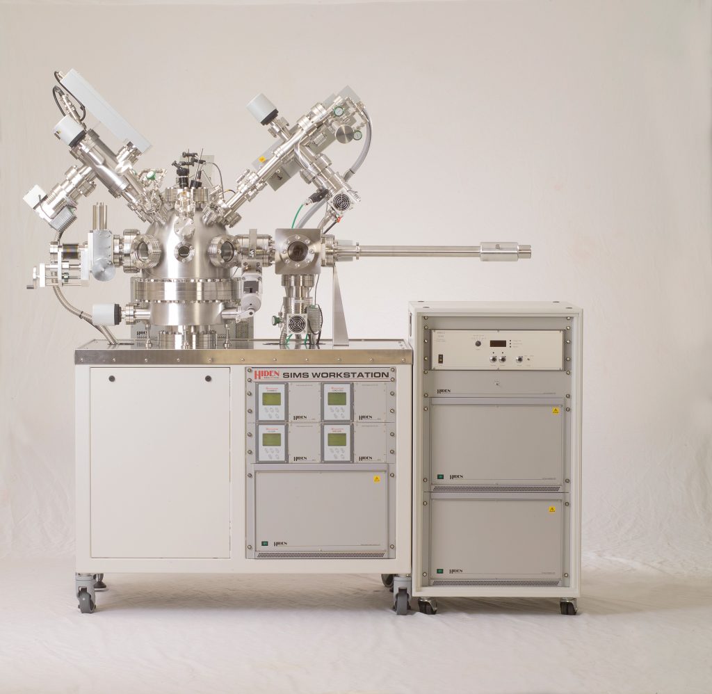
SIMS Workstation for depth profiling and surface analysis